Our Address
89, Asanvalley-ro, Dunpo-myeon, Asan-si, Chungcheongnam-do, Republic of Korea
Urgent issue? call us at
+82–41–546-5131
Technologies
- Home
- Technologies
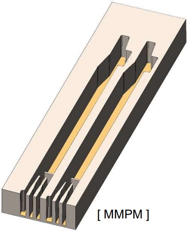
MMPM MEMS Technology Summary
MMPM (Micro-scale MEMS Point Mold)
MMPM technology is differentiated Point Engineering’s MEMS process which uses wafer-scale wet etchable material with high aspect ratio for mold for electroplating
in replace of photoresist to fabricate micro-scale MMPM features.
Vertically wet-etchable
▪ Micron-precision features within 1~2um of typical tolerance
Single mold layer thickness up to 120um
▪ Simplify MEMS electroplating process via max 120um thickness single mold
Enable precise patterning with high aspect ratio
▪ Extends the variety of shapes with max 20:1 of high aspect ratio
Excellent heat & chemical resistance properties
▪ Expand electroplatable metals (Au multi-layer)
▪ Optimal electroplating conditions for each metals.
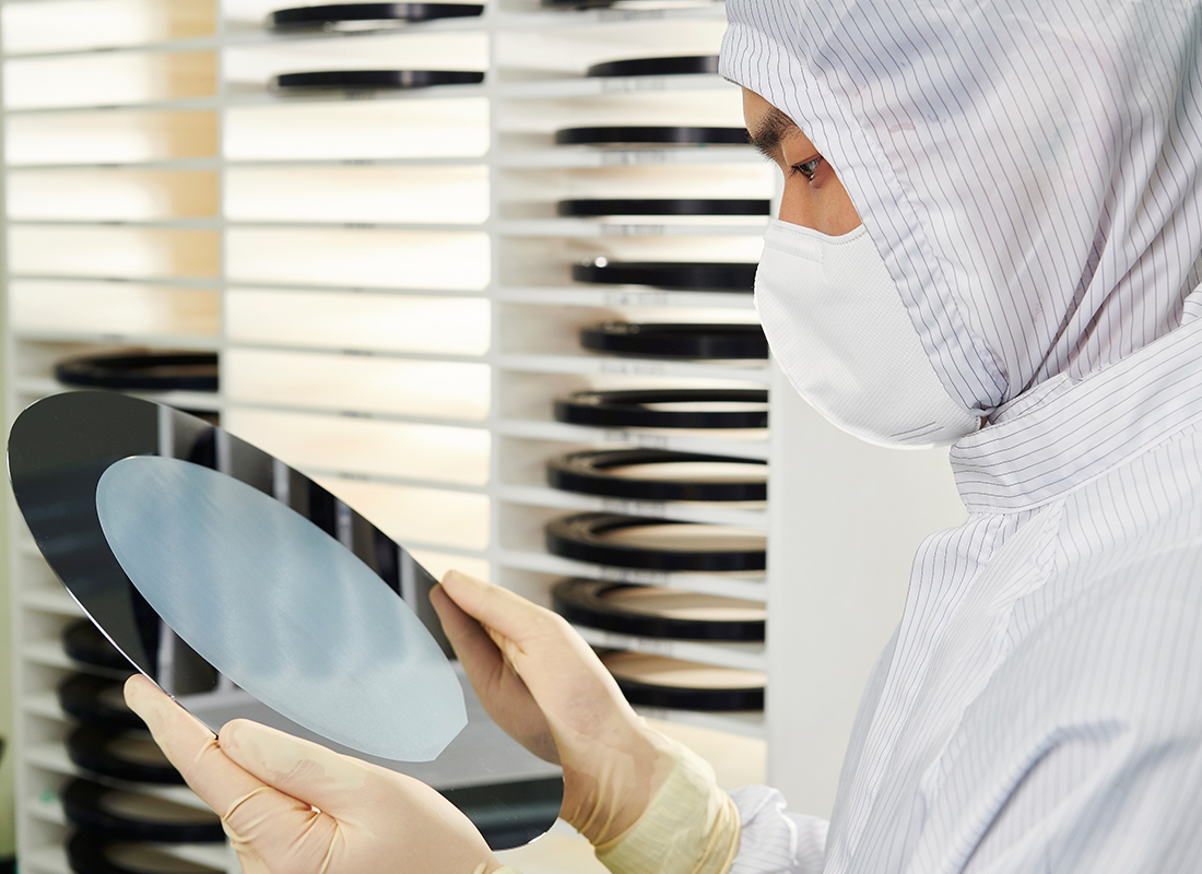
8’’ wafer-scale MEMS process possible
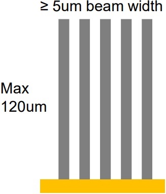
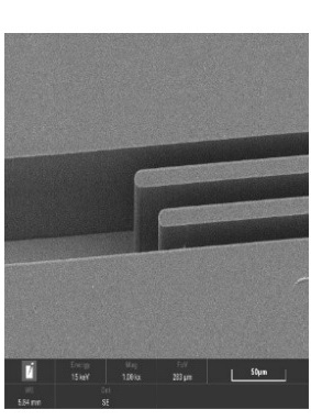
Advantages of MMPM Technology for MEMS
 High aspect ratio of MMPM enables finer & accurate feature
- Max 20:1 of Aspect ratio possible
(Recommended 15:1)
- Min 5um of line and space pattern possible
(Recommended ≥8um)
- Min 2um of corner radius pattern possible
- 1.0um of top-bottom deviation controllable
 Diverse metal selection options for optimum performance
- PdCo alloy / Au multi-layer
Cu-free electroplating for optimum high temp stability & signal stability
- PdCo alloy / Cu multi-layer for balanced hardness & high CCC
- NiCo alloy for best probe behavior
- Rhodium based tip for low wear & excellent contact resistance