Our Address
89, Asanvalley-ro, Dunpo-myeon, Asan-si, Chungcheongnam-do, Republic of Korea
Urgent issue? call us at
+82–41–546-5131
Technologies
- Home
- Technologies
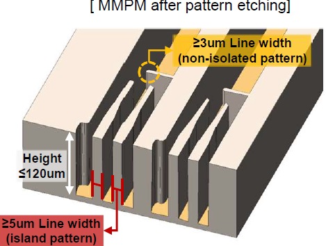
DESIGN RULES - MEMS buckling probe
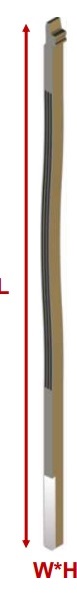
The layout design rules for the MMPM MEMS process are explained in following tables.
Following guidelines should be considered in design
| Category | Available Range | Recommended Range | |
|---|---|---|---|
| L | Total length | 1.5 ~ 6.0mm | 2.5 ~ 4.0mm |
| W | Width | ≥ 5um | 120*90um / 100*90um / 90*90um / 70*70um / 50*50um / 40*40um / 35*35um |
| H | Height | ≤ 120um | |
| - | Materials | Pd alloy/Au or Cu Ni alloy/Au or Cu |
Pd-co/Au for better signal & high temp stability |
| - | Options for distal ends |
Customized shape (Pointed, flat, etc) Rh plating on side, Au coating | |
| - | Options for buckling beam |
Insulation coating, Au coating | ※ Tolerance of probe’s critical dimension could be managed within ±2um (±1.5um controllable) |
| Category | Available Range | Recommended Range |
|---|---|---|
| Minimum beam
line & space width (for island or isolated pattern) |
≥ 5um | ≥ 8um |
| Minimum
line & space width (for non-isolated pattern) |
≥ 3um | ≥ 5um |
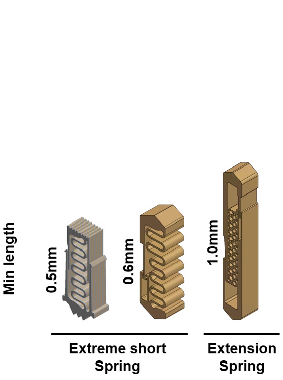
DESIGN RULES - MEMS Compression spring probe
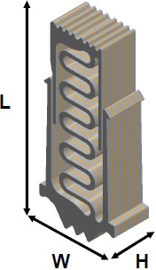
The layout design rules for the MMPM MEMS process are explained in following tables.
Following guidelines should be considered in design
| Category | Available Range | Recommended Range | |
|---|---|---|---|
| L | Total length | ≥ 0.5mm | 1.0 ~ 2.0mm |
| W | Width | ≥ 90um | ≥ 100um |
| H | Height | ≤ 120um | 35~90um |
| - | Materials | Pd alloy/Au or Cu, Ni alloy/Au or Cu | Ni alloy for cost competitiveness Pd-co/Au for better signal stability |
| - | Additional options | Customized shape (Pointed, flat, etc) Au coating (Whole, partial) | ※ Tolerance of probe’s critical dimension could be managed within ±2um (±1.5um controllable) |
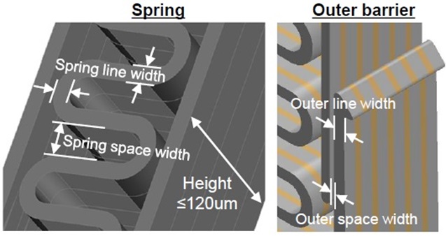
| Category | Available Range | Recommended Range |
|---|---|---|
| Miinimum spring line width | ≥ 5um | ≥ 8um |
| Minimum spring space width | ≥ 5um | ≥ 8um |
| Minimum outer barrier line width | ≥ 5um | ≥ 10μm (Prevent spring protrusion) |
| Minimum outer barrier space width | ≥ 5um | ≥ 8um |
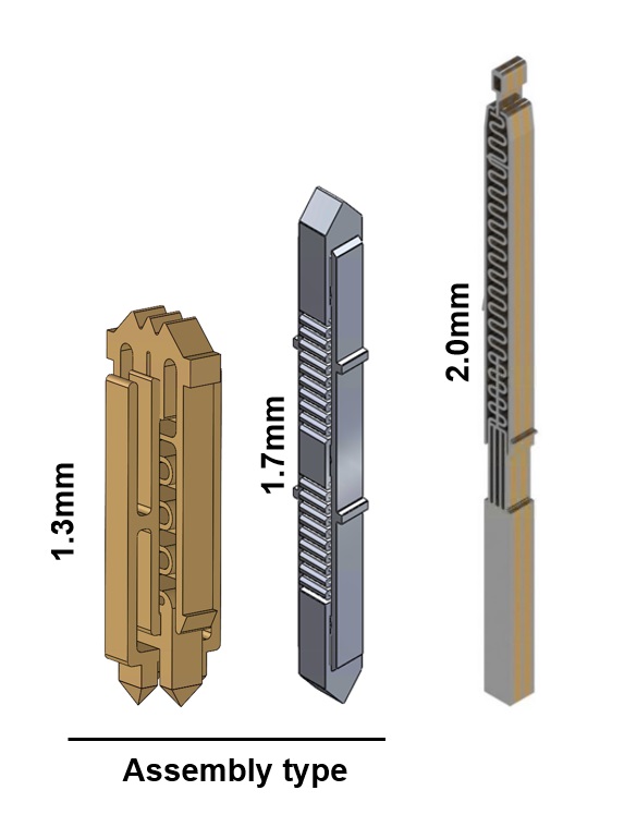
Expanding diversity in designs
Customized precision springs pins for wafer probing and fine-pitch socket application